LSN50v2 - LoRaWAN Sensor Node User Manual
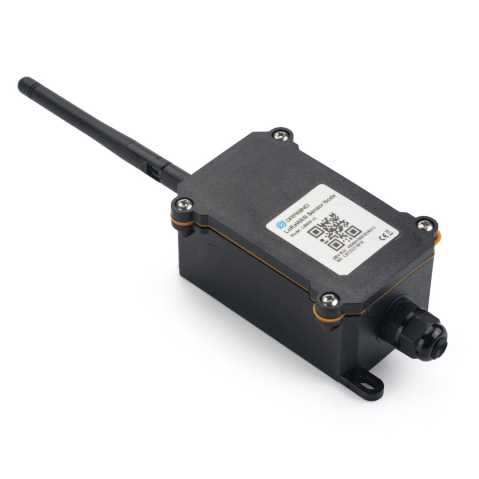
Table of Contents:
- 1. Introduction
- 2. Use LSN50v2 with LoRaWAN firmware
- 3. Using the AT Commands
- 4. Upload Firmware
- 5. Developer Guide
- 6. FAQ
- 6.1 Why there is 433/868/915 version?
- 6.2 What is the frequency range of LT LoRa part?
- 6.3 How to change the LoRa Frequency Bands/Region?
- 6.4 Can I use Private LoRa protocol?
- 6.5 How to set up LSN50v2 to work in 8 channel mode
- 6.6 How to set up LSN50v2 to work with Single Channel Gateway such as LG01/LG02?
- 6.7 How to configure the EUI keys in LSN50v2?
- 7. Trouble Shooting
- 8. Order Info
- 9. Packing Info
- 10. Support
- 11. References
1. Introduction
1.1 What is LSN50v2 LoRa Sensor Node
LSN50v2 is a Long Range LoRaWAN Sensor Node. It is designed for outdoor data logging and powered by Li/SOCl2 battery for long term use and secure data transmission. It is designed to facilitate developers to quickly deploy industrial level LoRa and IoT solutions. It helps users to turn the idea into a practical application and make the Internet of Things a reality. It is easy to program, create and connect your things everywhere.
It is based on SX1276/SX1278 allows the user to send data and reach extremely long ranges at low data-rates. It provides ultra-long range spread spectrum communication and high interference immunity whilst minimizing current consumption. It targets professional wireless sensor network applications such as irrigation systems, smart metering, smart cities, smartphone detection, building automation, and so on.
LSN50v2 uses STM32l0x chip from ST, STML0x is the ultra-low-power STM32L072xxxx microcontrollers incorporate the connectivity power of the universal serial bus (USB 2.0 crystal-less) with the high-performance ARM® Cortex®-M0+ 32-bit RISC core operating at a 32 MHz frequency, a memory protection unit (MPU), high-speed embedded memories (192 Kbytes of Flash program memory, 6 Kbytes of data EEPROM and 20 Kbytes of RAM) plus an extensive range of enhanced I/Os and peripherals.
LSN50v2 is an open source product, it is based on the STM32Cube HAL drivers and lots of libraries can be found in ST site for rapid development.
1.2 Specifications
Micro Controller:
- MCU: STM32L072xxxx
- Flash: 128KB
- RAM: 20KB
- EEPROM: 6KB
- Clock Speed: 32Mhz
Common DC Characteristics:
- Supply Voltage: 2.1v ~ 3.6v
- Operating Temperature: -40 ~ 85°C
- I/O pins: Refer to STM32L072 datasheet
LoRa Spec:
- Frequency Range,
- Band 1 (HF): 862 ~ 1020 Mhz
- or
- Band 2 (LF): 410 ~ 528 Mhz
- 168 dB maximum link budget.
- +20 dBm - 100 mW constant RF output vs.
- +14 dBm high efficiency PA.
- Programmable bit rate up to 300 kbps.
- High sensitivity: down to -148 dBm.
- Bullet-proof front end: IIP3 = -12.5 dBm.
- Excellent blocking immunity.
- Low RX current of 10.3 mA, 200 nA register retention.
- Fully integrated synthesizer with a resolution of 61 Hz .
- FSK, GFSK, MSK, GMSK, LoRaTM and OOK modulation.
- Built-in bit synchronizer for clock recovery.
- Preamble detection.
- 127 dB Dynamic Range RSSI.
- Automatic RF Sense and CAD with ultra-fast AFC.
- Packet engine up to 256 bytes with CRC.
- LoRaWAN 1.0.2 Specification
Battery:
- Li/SOCI2 un-chargeable battery
- Capacity: 4000mAh
- Self Discharge: <1% / Year @ 25°C
- Max continuously current: 130mA
- Max boost current: 2A, 1 second
Power Consumption
- STOP Mode: 2.7uA @ 3.3v
- LoRa Transmit Mode: 125mA @ 20dBm 44mA @ 14dBm
1.3 Features
- LoRaWAN 1.0.3 Class A, Class C
- STM32L072xxxx MCU
- SX1276/78 Wireless Chip
- Pre-load bootloader on USART1/USART2
- MDK-ARM Version 5.24a IDE
- I2C, LPUSART1, USB, SPI2
- 3x12bit ADC, 1x12bit DAC
- 20xDigital I/Os
- LoRa™ Modem
- Preamble detection
- Baud rate configurable
- CN470/EU433/KR920/US915/IN865
- EU868/AS923/AU915/MA869
- Open-source hardware / software
- Available Band:433/868/915/920 Mhz
- IP66 Waterproof Enclosure
- Ultra-Low Power consumption
- AT Commands to change parameters
- 8500mAh Battery for long term use。
1.4 Applications
- Smart Cities
- Smart Factory
- Smart Metering
- Smart Agriculture
- Smart Buildings & Home Automation
- Logistics and Supply Chain Management
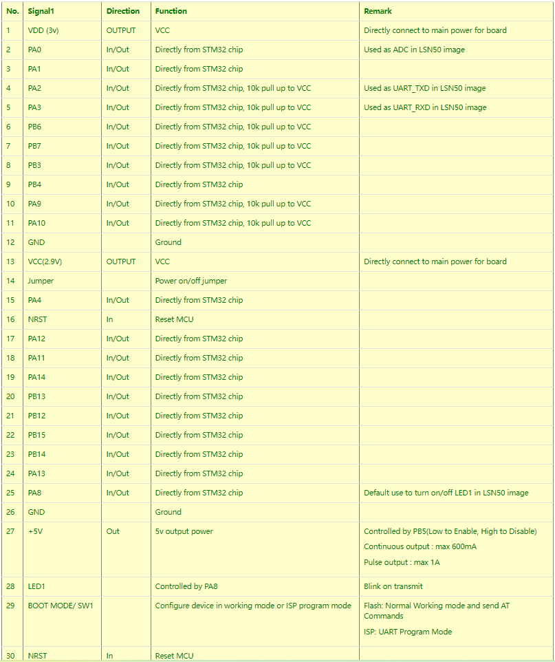
1.5 Pin Definitions and Switch
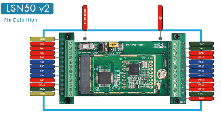
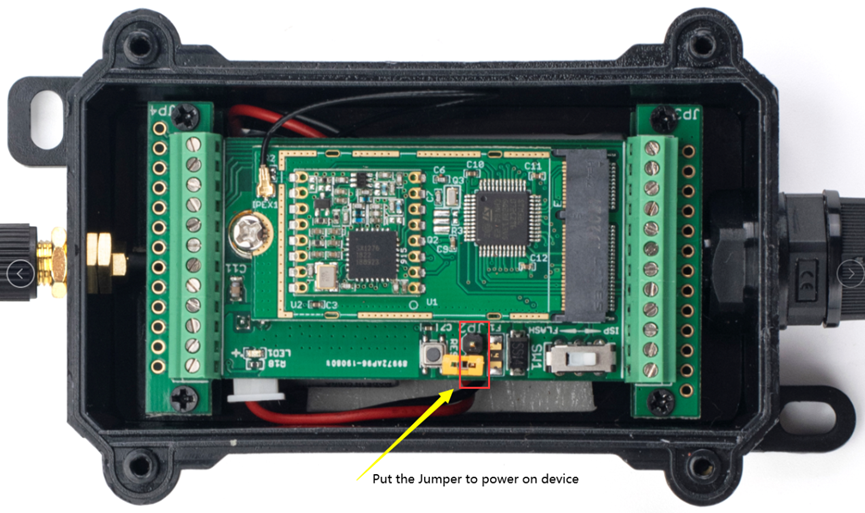
1.5.1 Jumper JP2
Power on Device when put this jumper.
1.5.2 BOOT MODE / SW1
1. ISP: upgrade mode, device won't have any signal in this mode. but ready for upgrade firmware. LED won't work. Firmware won't run.
2. Flash: work mode, device starts to work and send out console output for further debug
1.5.3 Reset Button
Press to reboot the device.
1.5.4 LED
It will flash:
1. When boot the device in flash mode
2. Send an uplink packet
1.6 Hardware Change log
Note: Hardware version is marked in the PCB.
LSN50v2 v2.1:
- Change R14 to 1M ohm
- Change R3, R4 to 4.7Kohm. So no need to modify them for 3 DS18B20 connection.
- Add ESD to each I/O
LSN50v2 v2.0:
- Change to a new enclosure. Improve with external antenna, IP68, ear hook.
2. Use LSN50v2 with LoRaWAN firmware
2.1 How it works
The LSN50v2 is pre-loaded with a firmware and is configured as LoRaWAN OTAA Class A mode by default. It has OTAA keys to join LoRaWAN network. To connect a local LoRaWAN network, you just need to input the OTAA keys in the LoRaWAN IoT server and power on the LSN50v2. It will automatically join the network via OTAA.
In case you can't set the OTAA keys in the LoRaWAN OTAA server, and you have to use the keys from the server, you can use AT Commands to set the keys in the LSN50v2.
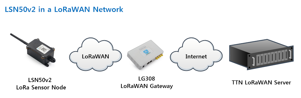
2.2 Quick guide to connect to LoRaWAN server (OTAA)
Following is an example for how to join the TTN V3 LoRaWAN Network. Below is the network structure; we use the LG308 as a LoRaWAN gateway in this example.
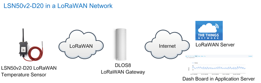
The LG308 is already set to connected to TTN V3 network , so what we need to now is configure the TTN V3 server.
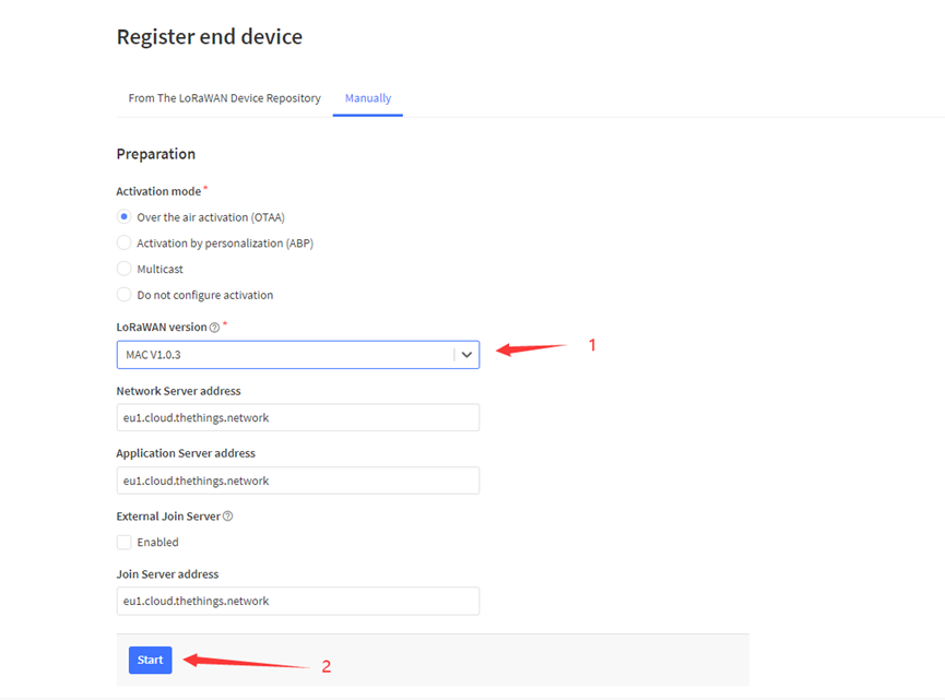
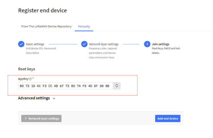
Step 1: Create a device in TTN with the OTAA keys from LSN50v2.
Each LSN50v2 is shipped with a sticker with the default device EUI as below:
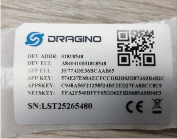
You can enter this key in the LoRaWAN Server portal. Below is TTN screen shot:
Register the device:
Add APP EUI and DEV EUI:
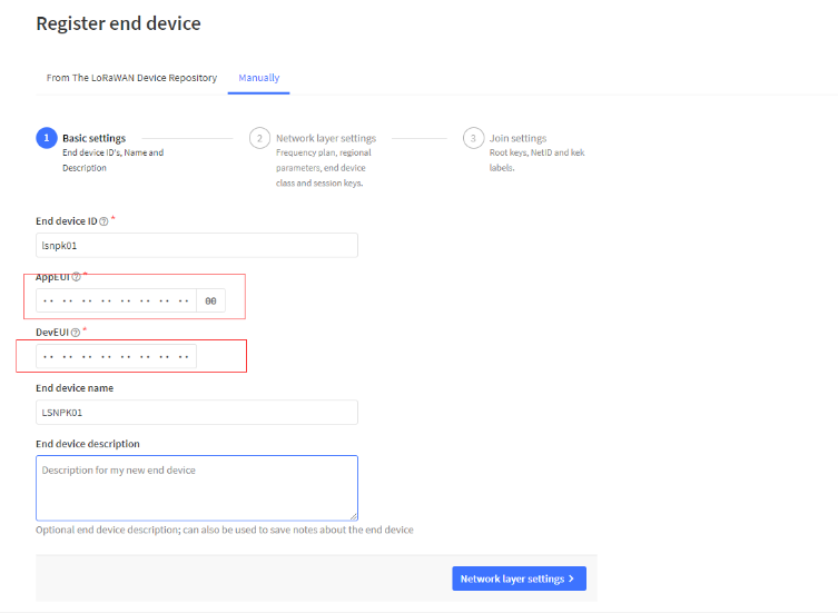
Add APP EUI in the application:
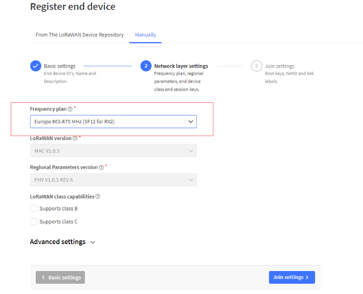
Add APP KEY
Step 2: Power on LSN50v2
Put a Jumper on JP2 to power on the device.
For LSn50v2:
Step 3: The LSN50v2 will auto join to the TTN V3 network. After join success, it will start to upload messages to TTN V3 and you can see the messages in the panel.
2.3 Working Mode & Uplink Payload
2.3.1 MOD=1 (Default Mode)
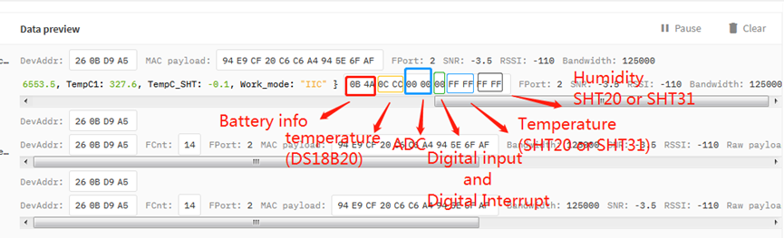
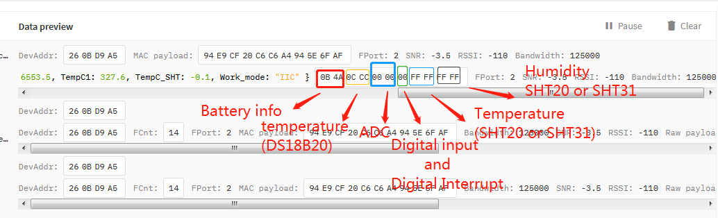
In this mode, uplink payload includes in total 11 bytes. Uplink packets use FPORT=2.

2.3.2 Decode payload in The Things Network
While using TTN V3 network, you can add the payload format to decode the payload.
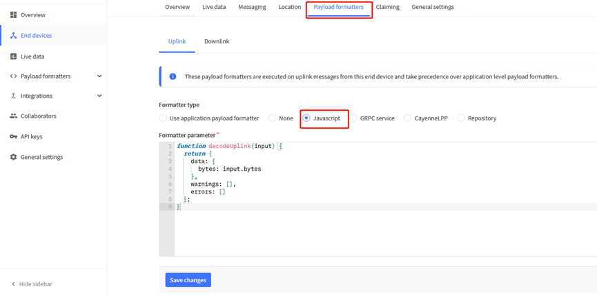
The payload decoder function for TTN V3 are here:
LSN50v2 TTN V3 Payload Decoder: https://github.com/dragino/dragino-end-node-decoder
2.4 Payload Explanation and Sensor Interface
2.4.1 Battery Info
Check the battery voltage for LSN50v2.
Ex1: 0x0B45 = 2885mV
Ex2: 0x0B49 = 2889mV
2.4.2 Digital Input
The digital input for pin PA12,
- When PA12 is high, the bit 1 of payload byte 6 is 1.
- When PA12 is low, the bit 1 of payload byte 6 is 0.
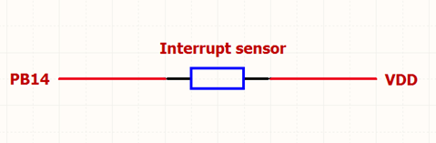
2.4.3 Digital Interrupt
Digital Interrupt refers to pin PB14, and there are different trigger methods. When there is a trigger, the LSN50v2 will send a packet to the server.
Interrupt connection method:
2.4.4 Distance Reading
Refer Ultrasonic Sensor section.
2.4.5 Battery Output - VDD pin
The VDD pin of LSN50v2 is connected to the Battery directly. If users want to use VDD pin to power an external sensor. User need to make sure the external sensor is of low power consumption. Because the VDD pin is always open. If the external sensor is of high power consumption. the battery of LSN50v2 will run out very soon.
2.4.6 +5V Output
Since v1.2 hardware version, a +5v output is added in the hardware. The +5V output will be valid for every sampling. LSN50v2 will enable +5V output before all sampling and disable the +5v after all sampling.
Since firmware v1.6.3, The 5V output time can be controlled by AT Command.
AT+5VT=1000
Means set 5V valid time to have 1000ms. So the real 5V output will actually have 1000ms + sampling time for other sensors.
By default the AT+5VT=500. If the external sensor which require 5v and require more time to get stable state, user can use this command to increase the power ON duration for this sensor.
2.5 Configure LSN50v2 via AT or Downlink
User can configure LSN50v2 via AT Commands or LoRaWAN Downlink Commands
There are two kinds of Commands:
- Common Commands: They should be available for each sensor, such as: change uplink interval, reset device. For firmware v1.7.0, user can find what common commands it supports: End Device AT Commands
- Sensor Related Commands: These commands are special designed for LSN50v2. User can see these commands below:
2.5.1 Common Commands:
They should be available for each of Dragino Sensors, such as: change uplink interval, reset device. For firmware v1.7.0, user can find what common commands it supports: End Device AT Commands
2.6 Firmware Change Log
Firmware download: https://www.dropbox.com/sh/9k0a6sn8a94dc03/AAD54woDmnmAMUMY2WfKfjxoa?dl=0
Firmware Change Log: https://www.dropbox.com/sh/9k0a6sn8a94dc03/AAD54woDmnmAMUMY2WfKfjxoa?dl=0
2.7 Use VDD or +5V to Power External Sensor
User can use VDD or +5V to power external sensor.
Note:
VDD is 2.5~3.3v from the battery + diode, the VDD is always on, so when use VDD to power external sensor, make sure the sensor has a low power consumption in sleep mode ( less 50 uA) to get a long battery life.
+5V output is only ON when sampling. And MCU will turn off it after sampling. So if sensor can support 5v, +5V out is the best choice. See here for more info.
Note: Always test the actually current pass by the JP2 jumper when connect to a new type of sensor.
2.8 Battery Analysis
2.8.1 Battery Type
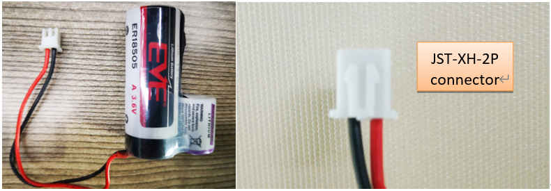
The LSN50v2 battery is a combination of a 4000mAh or 8500mAh Li/SOCI2 Battery and a Super Capacitor. The battery is non-rechargeable battery type with a low discharge rate (<2% per year). This type of battery is commonly used in IoT devices such as water meter.
The battery is designed to last for more than 5 years for the LSN50v2.
The battery related documents as below:
- Battery Dimension,
- Lithium-Thionyl Chloride Battery datasheet, Tech Spec
- Lithium-ion Battery-Capacitor datasheet, Tech Spec
2.8.3 Battery Note
The Li-SICO battery is designed for small current / long period application. It is not good to use a high current, short period transmit method. The recommended minimum period for use of this battery is 5 minutes. If you use a shorter period time to transmit LoRa, then the battery life may be decreased.
2.8.4 Replace the battery
You can change the battery in the LSN50v2.The type of battery is not limited as long as the output is between 3v to 3.6v. On the main board, there is a diode (D1) between the battery and the main circuit. If you need to use a battery with less than 3.3v, please remove the D1 and shortcut the two pads of it so there won’t be voltage drop between battery and main board.
The default battery pack of LSN50v2 includes a ER18505 plus super capacitor. If user can't find this pack locally, they can find ER18505 or equivalence, which will also work in most case. The SPC can enlarge the battery life for high frequency use (update period below 5 minutes).
3. Using the AT Commands
3.1 Access AT Commands
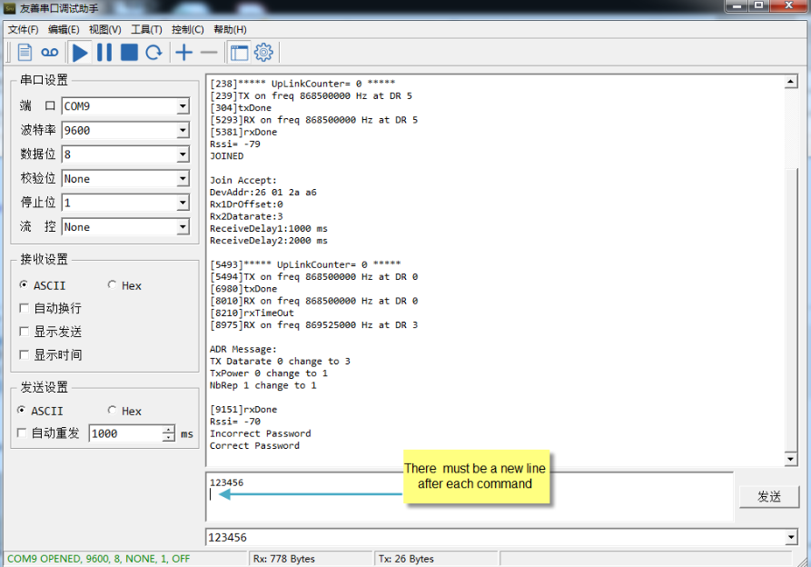
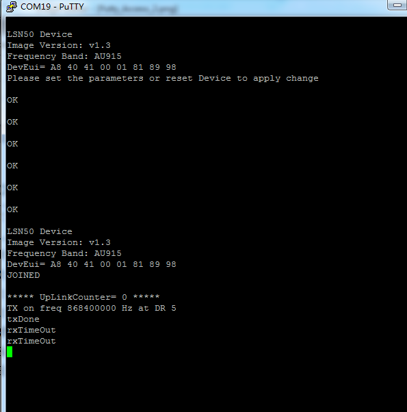
LSN50v2 supports AT Command set in the stock firmware. You can use a USB to TTL adapter to connect to LSN50v2 for using AT command, as below.
LSN50v2 UART connection photo
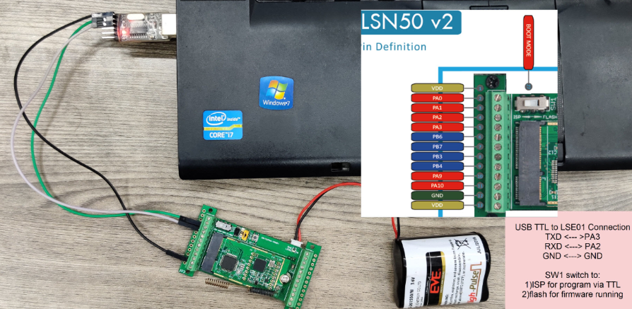
In the PC, you need to set the serial baud rate to 9600 to access the serial console for LSN50v2. LSN50v2 will output system info once power on as below:
3.2 Common AT Command Sequence
3.2.1 Multi-channel ABP mode (Use with SX1301/LG308)
If device has not joined network via OTAA:
AT+FDR
AT+NJM=0
ATZ
If device already joined network:
AT+NJM=0
ATZ
3.2.2 Single-channel ABP mode (Use with LG01/LG02)
See Sect 6.7
4. Upload Firmware
Notes:
- Since image v1.3, the firmware will show version info during boot. If your device doesn't show version info, you may have a very old image version.
- Always run AT+FDR to reset parameters to factory default after an update image.
If the update is from image >= v1.3 to another image version >=v1.3, then the keys will be kept after running AT+FDR.
Otherwise (e.g. from v1.2 to v1.3), AT+FDR may erase the keys.
4.1 Upload Firmware via Serial Port
The LSN50v2's AT Command port can be used for firmware upgrade. The hardware connection for upgrade firmware is as below:
Step1: Download flash loader.
Step2: Download the LSN50v2 Image files.
Step3: Open flashloader; choose the correct COM port to update
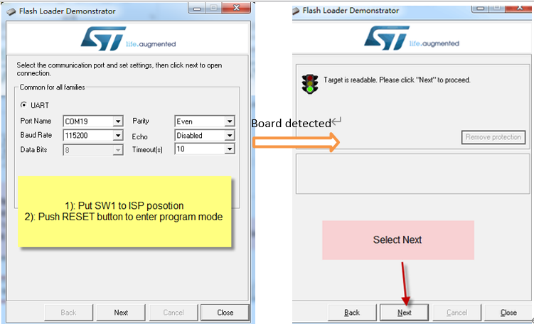
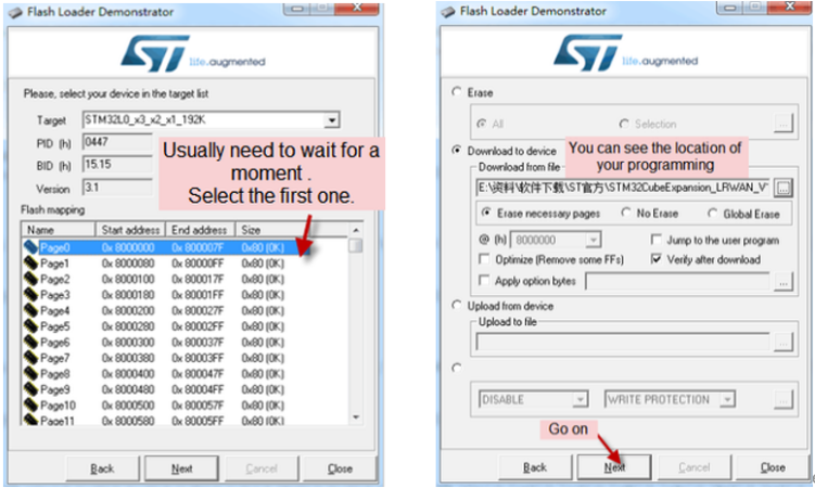
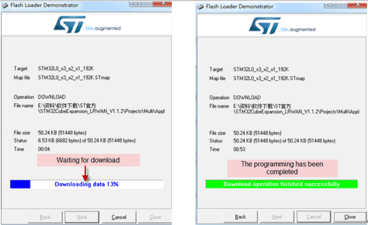
Step4: Switch SW1 back to flash state and push the RESET button.
The LSN50v2 will then run the new firmware.
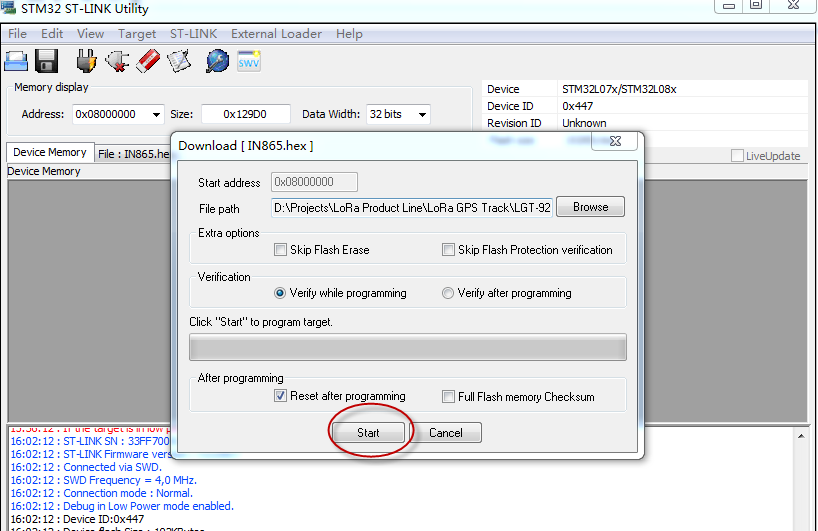
4.2 Upload Firmware via ST-Link V2
You can use ST-LINK to upgrade firmware into LSN50v2. The hardware connection for upgrade firmware is as below:
Connection:
- ST-LINK v2 GND <--> LSN50v2 GND
- ST-LINK v2 SWCLK <--> LSN50v2 PA14
- ST-LINK v2 SWDIO <--> LSN50v2 PA13
- ST-LINK v2 RST <--> LSN50v2 NRST
Step1: Install ST-LINK driver first and then install ST-LINK Utility
Step2: Download the LSN50v2 Image files.
Step3: Open ST-LINK utility, file --> open file to select the image to be upgraded.
Step4: Click the “Program Verify” button on ST-LINK.
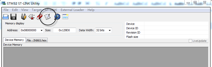
Step5: The led on the ST-LINK adapter will now blinking, and the ST-Link utility will pop up a download window. Click the start button to download the image to LSN50v2.
NOTE: If this step fails, ST-LINK can't establish connection to LSN50v2, please try to swap SWDIO & SWCLK pin. Some ST-LINK v2 devices are incorrectly marked.
5. Developer Guide
Software Source Code Download : https://github.com/dragino/LoRa_STM32/tree/master/STM32CubeExpansion_LRWAN
Hardware Source Code Download: https://github.com/dragino/Lora/tree/master/LSN50
LSN50 is an open source project, developer can use compile their firmware for customized applications. User can get the source code from:
Software Source Code: https://github.com/dragino/LoRa_STM32/tree/master/STM32CubeExpansion_LRWAN
Hardware Design files: https://github.com/dragino/Lora/tree/master/LSN50
Use Keil to open project file:
STM32CubeExpansion_LRWAN/Projects/Multi/Applications/LoRa/DRAGINO-LRWAN(AT)/MDK-ARM/STM32L072CZ-Nucleo/Lora.uvprojx
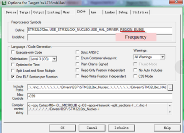
In Keil, you can see what frequency band the code support.
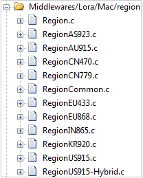
1. If you want to change frequency, modify the Preprocessor Symbols.
For example, change EU868 to US915
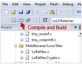
2. Compile and build
6. FAQ
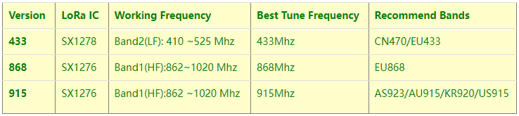
6.1 Why there is 433/868/915 version?
Different countries have different rules for the ISM band for LoRa. Although the LoRa chip can support a wide range of Frequencies, we provide different versions of the hardware for best tune of the LoRa hardware part.
6.2 What is the frequency range of LT LoRa part?
Different LT version supports different frequency range, below is the table for the working frequency and recommend bands for each model:
6.3 How to change the LoRa Frequency Bands/Region?
You can follow the instructions for how to upgrade image.
When downloading the images, choose the required image file for download.
6.4 Can I use Private LoRa protocol?
The stock firmware is based on LoRaWAN protocol. You can use a private LoRa protocol in LSN50v2. This section describes an example for base LoRa transfer. It is a reference/demo and we do not provide further software development support on this topic.
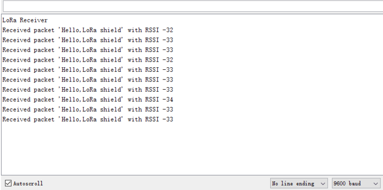
In this demo, we will show the communication between LoRa Shield and LSN50v2, both of them using the basic LoRa library. LSN50v2 will send a message to a LoRa Shield and the LoRa Shield will print it to the console.
LoRa Shield + UNO:
Use the LoRa Library and upload the LoRa Receive Sketch to Arduino.
Refs: https://www.dropbox.com/sh/u9s41qdx5yujwcb/AAAT5r4QkMaeOogWrzJt7Wn4a?dl=0
Open the serial monitor to Arduino. The device acts as a LoRa Receiver and listen on the frequency 868.3Mhz by default.
LSN50v2:
Use the <LoRa RAW code> . The project file is in: MDK-ARM\STM32L072CZ-Nucleo\ Lora.uvprojx
Compile it and Upload it to LSN50v2, the LSN50v2 will transfer on the frequency 868.3Mhz.
In the Arduino Console, it will see the received packets as below.
6.5 How to set up LSN50v2 to work in 8 channel mode
By default, the frequency bands US915, AU915, CN470 work in 72 frequencies. Many gateways are 8 channel gateways, and in this case, the OTAA join time and uplink schedule is long and unpredictable while the end node is hopping in 72 frequencies.
You can configure the end node to work in 8 channel mode by using the AT+CHE command. The 500kHz channels are always included for OTAA.
For example, in US915 band, the frequency table is as below. By default, the end node will use all channels (0~71) for OTAA Join process. After the OTAA Join, the end node will use these all channels (0~71) to send uplink packets.
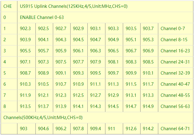
When you use the TTN V3 network, the US915 frequency bands use are:
903.9 - SF7BW125 to SF10BW125
904.1 - SF7BW125 to SF10BW125
904.3 - SF7BW125 to SF10BW125
904.5 - SF7BW125 to SF10BW125
904.7 - SF7BW125 to SF10BW125
904.9 - SF7BW125 to SF10BW125
905.1 - SF7BW125 to SF10BW125
905.3 - SF7BW125 to SF10BW125
904.6 - SF8BW500
Because the end node is now hopping in 72 frequency, it makes it difficult for the devices to Join the TTN V3 network and uplink data. To solve this issue, you can access the device via the AT commands and run:
AT+CHE=2
ATZ
to set the end node to work in 8 channel mode. The device will work in Channel 8-15 & 64-71 for OTAA, and channel 8-15 for Uplink.
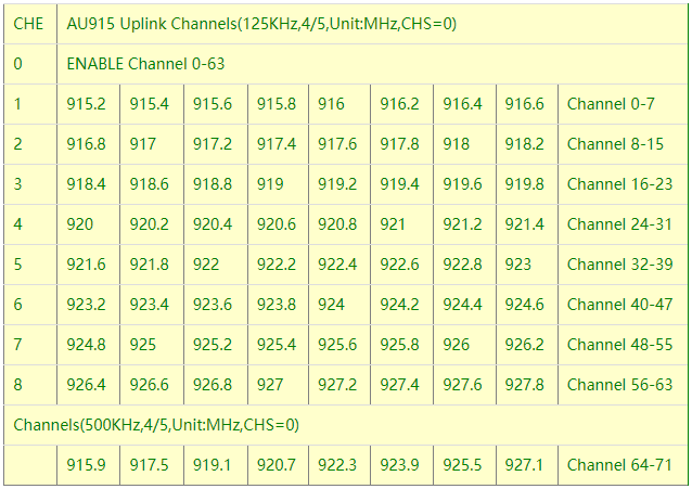
The AU915 band is similar. Below are the AU915 Uplink Channels.
6.6 How to set up LSN50v2 to work with Single Channel Gateway such as LG01/LG02?
In this case, users need to set LSN50v2 to work in ABP mode and transmit in only one frequency.
Assume we have a LG02 working in the frequency 868400000 now, below is the steps.
Step1: Log in TTN V3, Create an ABP device in the application and input the network session key (NETSKEY), app session key (APPSKEY) from the device.
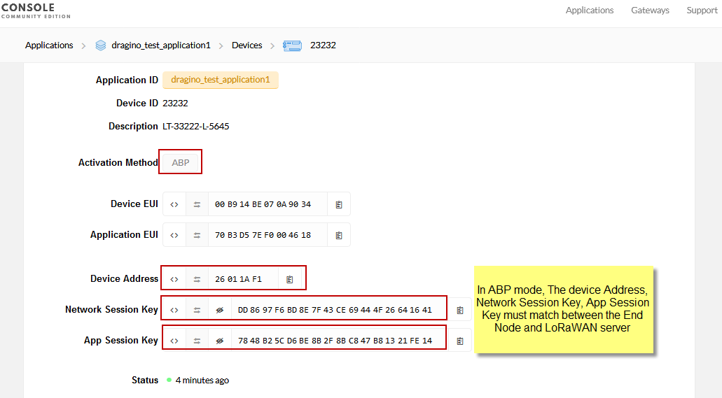
Note: You need to make sure the above three keys match in the device and in TTN V3. You can change them either in TTN V3 or in the Device to make them match. In TTN V3, NETSKEY and APPSKEY can be configured in the setting page, but the Device Addr is generated by TTN V3.
You can also change the Device ADDR in TTN V3 by using the The Things Network CLI.
Step2: Run AT commands to make the LSN50v2 work in Single frequency and ABP mode. Below are the AT commands:
AT+FDR : Reset Parameters to Factory Default, Keys Reserve
AT+NJM=0 : Set to ABP mode
AT+ADR=0 : Set the Adaptive Data Rate Off
AT+DR=5 : Set Data Rate (Set AT+DR=3 for 915 band)
AT+TDC=300000 : Set transmit interval to 5 minutes
AT+CHS=868400000 : Set transmit frequency to 868.4Mhz
AT+DADDR=26 01 1A F1 :Set Device Address to 26 01 1A F1
ATZ : Reset MCU
As shown below:
6.7 How to configure the EUI keys in LSN50v2?
The early version of LSN50v2 firmware doesn't have pre-configured keys.
It is recommended that you update the image to the latest version before configure the keys. Refer upgrade_image to update the firmware to the latest version.
Run AT commands to set the keys to desired keys; refer AT Command manual.
7. Trouble Shooting
7.1 Connection problem when uploading firmware.
Issue: While using USB to TTL to upload firmware via UART interface. It works for several times but most of times it fails.
Checklist:
1. Double check if follow up exactly the steps as manual.
2. Check if hardware works fine: a) check if AT command works, b) check if ISP / flash switch works: PA12 will have different output level while set the ISP/Flash Switch in different position. c) check if reset button works.
3. If you use Windows10 system. Please change the flash loader to run in Windows7 compatibility mode.
4. We have seen cases where the FT232 USB TTL adapter has a reliability issue with the PC USB chipset (Intel). In this case, even though points 1 and 2 above work, it still has a reliability issue for uploading. If this happens, change to a different PC or change the USB to TTL adapter to solve the issue.
7.2 Why I can't join TTN V3 in US915 / AU915 bands?
It is due to channel mapping. Please see the Eight Channel Mode section above for details.
7.3 AT Command input doesn't work
In the case if user can see the console output but can't type input to the device. Please check if you already include the ENTER while sending out the command. Some serial tool doesn't send ENTER while press the send key, user need to add ENTER in their string.
8. Order Info
Part Number: LSN50v2-XX-YY-ZZ
XX: The default frequency band
- AS923 : LoRaWAN AS923 band
- AU915 : LoRaWAN AU915 band
- EU433 : LoRaWAN EU433 band
- EU868 : LoRaWAN EU868 band
- KR920 : LoRaWAN KR920 band
- US915 : LoRaWAN US915 band
- IN865 : LoRaWAN IN865 band
- CN470 : LoRaWAN CN470 band
YY: Hole Option
- 12: With M12 waterproof cable hole
- 16: With M16 waterproof cable hole
- 20: With M20 waterproof cable hole (LSN50v2 doesn't have this version)
- NH: No Hole
ZZ: Battery Option ( Only valid for v2 model)
- 4: with 4000mAh battery
- 8: with 8500mAg battery
9. Packing Info
For LSN50v2:
Package Includes:
- LSN50v2 LoRa Sensor Node x 1
- External antenna x 1
- Spring Antenna (evaluate purpose)
Dimension and weight:
- Device Size: 9.7 x 6.5 x 4.7 cm
- Device Weight: 150g
- Package Size / pcs : 14.0 x 8x 5 cm
- Weight / pcs : 180g
10. Support
- Support is provided Monday to Friday, from 09:00 to 18:00 GMT+8. Due to different timezones we cannot offer live support. However, your questions will be answered as soon as possible in the before-mentioned schedule.
- Provide as much information as possible regarding your enquiry (product models, accurately describe your problem and steps to replicate it etc) and send a mail to support@dragino.com.
11. References